

Date:15/11/16
 Scientists have developed the first semiconductor-free, optically-controlled microelectronic device which conducts 1,000 per cent more electricity than conventional electronic devices. The discovery paves the way for microelectronic devices that are faster and capable of handling more power, and could also lead to more efficient solar panels.
Using metamaterials, engineers at the University of California San Diego in the US were able to build a microscale device that shows a 1,000 per cent increase in conductivity when activated by low voltage and a low power laser. The capabilities of existing microelectronic devices, such as transistors, are ultimately limited by the properties of their constituent materials, such as their semiconductors, researchers said.
For example, semiconductors can impose limits on a device’s conductivity, or electron flow. Semiconductors have what is called a band gap, meaning they require a boost of external energy to get electrons to flow through them. Electron velocity is limited, since electrons are constantly colliding with atoms as they flow through the semiconductor.
A team of researchers led by Dan Sievenpiper at UC San Diego sought to remove these roadblocks to conductivity by replacing semiconductors with free electrons in space. “And we wanted to do this at the microscale,” said Ebrahim Forati, a former postdoctoral researcher in Sievenpiper’s lab and first author of the study.
However, liberating electrons from materials is challenging. It either requires applying high voltages (at least 100 Volts), high power lasers or extremely high temperatures (more than 538 degrees Celsius), which are not practical in micro- and nanoscale electronic devices.
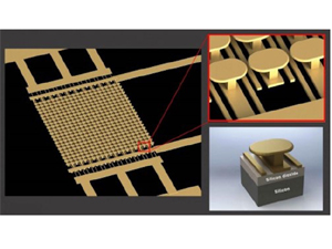
To address this challenge, Sievenpiper’s team fabricated a microscale device that can release electrons from a material without such extreme requirements. The device consists of an engineered surface, called a metasurface, on top of a silicon wafer, with a layer of silicon dioxide in between.
The metasurface consists of an array of gold mushroom-like nanostructures on an array of parallel gold strips. The gold metasurface is designed such that when a low DC voltage (under 10 Volts) and a low power infrared laser are both applied, the metasurface generates “hot spots” – spots with a high intensity electric field – that provide enough energy to pull electrons out from the metal and liberate them into space.
Tests on the device showed a 1,000 per cent change in conductivity. “That means more available electrons for manipulation,” Ebrahim said. The research was published in the journal Nature Communications.
Semiconductor-free microelectronic device allows high power
 Scientists have developed the first semiconductor-free, optically-controlled microelectronic device which conducts 1,000 per cent more electricity than conventional electronic devices. The discovery paves the way for microelectronic devices that are faster and capable of handling more power, and could also lead to more efficient solar panels.
Using metamaterials, engineers at the University of California San Diego in the US were able to build a microscale device that shows a 1,000 per cent increase in conductivity when activated by low voltage and a low power laser. The capabilities of existing microelectronic devices, such as transistors, are ultimately limited by the properties of their constituent materials, such as their semiconductors, researchers said.
For example, semiconductors can impose limits on a device’s conductivity, or electron flow. Semiconductors have what is called a band gap, meaning they require a boost of external energy to get electrons to flow through them. Electron velocity is limited, since electrons are constantly colliding with atoms as they flow through the semiconductor.
A team of researchers led by Dan Sievenpiper at UC San Diego sought to remove these roadblocks to conductivity by replacing semiconductors with free electrons in space. “And we wanted to do this at the microscale,” said Ebrahim Forati, a former postdoctoral researcher in Sievenpiper’s lab and first author of the study.
However, liberating electrons from materials is challenging. It either requires applying high voltages (at least 100 Volts), high power lasers or extremely high temperatures (more than 538 degrees Celsius), which are not practical in micro- and nanoscale electronic devices.
To address this challenge, Sievenpiper’s team fabricated a microscale device that can release electrons from a material without such extreme requirements. The device consists of an engineered surface, called a metasurface, on top of a silicon wafer, with a layer of silicon dioxide in between.
The metasurface consists of an array of gold mushroom-like nanostructures on an array of parallel gold strips. The gold metasurface is designed such that when a low DC voltage (under 10 Volts) and a low power infrared laser are both applied, the metasurface generates “hot spots” – spots with a high intensity electric field – that provide enough energy to pull electrons out from the metal and liberate them into space.
Tests on the device showed a 1,000 per cent change in conductivity. “That means more available electrons for manipulation,” Ebrahim said. The research was published in the journal Nature Communications.
Views: 551
©ictnews.az. All rights reserved.Similar news
- The mobile sector continues its lead
- Facebook counted 600 million active users
- Cell phone testing laboratory is planned to be built in Azerbaijan
- Tablets and riders outfitted quickly with 3G/4G modems
- The number of digital TV channels will double to 24 units
- Tax proposal in China gets massive online feedback
- Malaysia to implement biometric system at all entry points
- Korea to build Green Technology Centre
- Cisco Poised to Help China Keep an Eye on Its Citizens
- 3G speed in Azerbaijan is higher than in UK
- Government of Canada Announces Investment in Green Innovation for Canada
- Electric cars in Azerbaijan
- Dominican Republic Govt Issues Cashless Benefits
- Spain raises €1.65bn from spectrum auction
- Camden Council boosts mobile security


