

Date:11/02/19
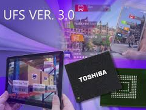
 Toshiba announced the industry’s first embedded flash chips to use the ultra-fast Universal Flash Storage (UFS) version 3.0 technology. The new memory chips target smartphones, tablets, and augmented/virtual reality systems.
Toshiba said that the new chips use the cutting-edge 96-layer BiCS FLASH, the company’s 3D flash memory technology, and a controller in a JEDEC-standard 11.5 x 13mm package. Chips will be made available in three capacities: 128GB, 256GB, and 512GB.
The controller performs error correction, wear leveling, logical-to-physical address translation, and bad-block management for simplified system development.
All three devices are compliant with JEDEC UFS 3.0, as well as the HS-GEAR4 standard, which has a theoretical interface speed of up to 11.6 Gigabits per second per lane. With two lanes, the chips can reach a peak interface bandwidth of 23.2Gbps (2.9GB/s).
Toshiba didn’t disclose the read and write speed of the chips, but it noted that the 512GB drives will support an increased read and write performance over the previous generation of 70 percent and 80 percent, respectively.
Toshiba is no stranger to JEDEC’s UFS memory standard, as it was also the first company to release UFS samples back in 2013, just as now, six years later, it’s the first to sample UFS 3.0 embedded memory chips.
The UFS standard has started to gain rapid adoption in smartphones over the past few years, as a higher-performance alternative to eMMC. Samsung and other companies have even started to use the standard for external memory cards, as an alternative to SD cards.
Smartphones using Toshiba’s 128GB chip are expected to ship later this year.
Toshiba Unveils Industry’s First UFS Ver. 3.0 Embedded Flash Memory Devices
 Toshiba announced the industry’s first embedded flash chips to use the ultra-fast Universal Flash Storage (UFS) version 3.0 technology. The new memory chips target smartphones, tablets, and augmented/virtual reality systems.
Toshiba said that the new chips use the cutting-edge 96-layer BiCS FLASH, the company’s 3D flash memory technology, and a controller in a JEDEC-standard 11.5 x 13mm package. Chips will be made available in three capacities: 128GB, 256GB, and 512GB.
The controller performs error correction, wear leveling, logical-to-physical address translation, and bad-block management for simplified system development.
All three devices are compliant with JEDEC UFS 3.0, as well as the HS-GEAR4 standard, which has a theoretical interface speed of up to 11.6 Gigabits per second per lane. With two lanes, the chips can reach a peak interface bandwidth of 23.2Gbps (2.9GB/s).
Toshiba didn’t disclose the read and write speed of the chips, but it noted that the 512GB drives will support an increased read and write performance over the previous generation of 70 percent and 80 percent, respectively.
Toshiba is no stranger to JEDEC’s UFS memory standard, as it was also the first company to release UFS samples back in 2013, just as now, six years later, it’s the first to sample UFS 3.0 embedded memory chips.
The UFS standard has started to gain rapid adoption in smartphones over the past few years, as a higher-performance alternative to eMMC. Samsung and other companies have even started to use the standard for external memory cards, as an alternative to SD cards.
Smartphones using Toshiba’s 128GB chip are expected to ship later this year.
Views: 309
©ictnews.az. All rights reserved.Similar news
- Azerbaijani project to monitor disease via mobile phones
- Innovative educational system to be improved under presidential decree
- NTRC prolongs license of two TV and radio organizations for 6 years
- Azerbaijan establishes e-registry for medicines
- Azerbaijani museum introduces e-guide
- Nar Mobile opens “Nar Dunyasi” sales and service center in Siyazan city
- International conference on custom electronic services held in Baku
- OIC secretary general to attend COMSTECH meeting in Baku
- Azerbaijan develops earthquake warning system
- New law to regulate transition to digital broadcasting in Azerbaijan
- Azerbaijani State Social Protection Fund introduces electronic digital signature
- Intellectual traffic management system in Baku to be commissioned in December
- Tax Ministry of Azerbaijan started receiving video-addresses
- World Bank recommends Azerbaijan to speed up e-service introduction in real estate
- Azerbaijan to shift to electronic registration of real estate


