

Date:02/06/21
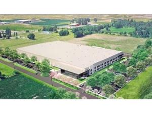
 Hitachi High-Tech Corporation and Hitachi High-Tech Group company, Hitachi High-Tech America, Inc., announce today the establishment of Hitachi’s Center of Excellence in Portland, a new centralized facility for semiconductor engineering in Hillsboro, Oregon.
We are consolidating our semiconductor technology development facilities in the United States into this newly established facility. At this new location, we will partner with our customers in the semiconductor industry to jointly create new Lumada solutions that lead to improved customer value by utilizing Hitachi’s advanced digital technology. Our goal is to support our customers utilizing Hitachi’s unique technology innovations, contribute to solving their technology challenges, and partner on management-related challenges.
Due to the expanded implementation of AI and IoT, as well as the emergence of 5G compatible digital devices, the amount of data used in communication has been increasing exponentially. Consequently, capital investment in data centers and base stations that support such data transmission is accelerating. Demand for semiconductor devices for automobiles, such as EVs (electric vehicles), and autonomous driving technology is also growing. As a result, the semiconductor device market is expected to continue growing and expanding into the near future. Our customers require continuous and uninterrupted technology innovation in order to support this market expansion. In addition, Hitachi High-Tech Group’s goal is to solve technology issues related to scaling, multi-layering, and leading-edge 3D memory and logic devices (including FinFETs and gate-all-around architectures) while partnering with our customers on business management challenges.
Hitachi High-Tech America originally established the Process Engineering Center in Hillsboro, Oregon in 2014. This overseas facility has been supporting R&D and production projects for our US-based customers in the semiconductor etch field. In order to add to those efforts in the United States, where further growth is expected in advanced semiconductor technology development, Hitachi High-Tech America will consolidate and expand its technology development capabilities at this new facility in Hillsboro, Oregon. Hitachi High-Tech Group will accelerate the implementation of collaborative programs to shorten development turnaround time and improve productivity and yield during each semiconductor manufacturing phase.
The new facility has a reinforced concrete two-story structure and is scheduled to be completed in August 2022. It provides a collaboration area where we can work closely with customers to jointly create solutions. As one of the key initiatives of Hitachi, Ltd.’s Lumada solution, the site will utilize our latest process, inspection, measurement, and analysis systems based on Hitachi High-Tech Group’s core technologies for “Observation, Measurement, and Analysis” and Hitachi, Ltd.’s IT and OT (operational technology) technologies to create these unique solutions.
Hitachi High-Tech Group will continue to pursue and create new social and environmental value together with our customers and contribute to cutting-edge manufacturing.
Hitachi establishes centralized semiconductor engineering facility in Oregon
 Hitachi High-Tech Corporation and Hitachi High-Tech Group company, Hitachi High-Tech America, Inc., announce today the establishment of Hitachi’s Center of Excellence in Portland, a new centralized facility for semiconductor engineering in Hillsboro, Oregon.
We are consolidating our semiconductor technology development facilities in the United States into this newly established facility. At this new location, we will partner with our customers in the semiconductor industry to jointly create new Lumada solutions that lead to improved customer value by utilizing Hitachi’s advanced digital technology. Our goal is to support our customers utilizing Hitachi’s unique technology innovations, contribute to solving their technology challenges, and partner on management-related challenges.
Due to the expanded implementation of AI and IoT, as well as the emergence of 5G compatible digital devices, the amount of data used in communication has been increasing exponentially. Consequently, capital investment in data centers and base stations that support such data transmission is accelerating. Demand for semiconductor devices for automobiles, such as EVs (electric vehicles), and autonomous driving technology is also growing. As a result, the semiconductor device market is expected to continue growing and expanding into the near future. Our customers require continuous and uninterrupted technology innovation in order to support this market expansion. In addition, Hitachi High-Tech Group’s goal is to solve technology issues related to scaling, multi-layering, and leading-edge 3D memory and logic devices (including FinFETs and gate-all-around architectures) while partnering with our customers on business management challenges.
Hitachi High-Tech America originally established the Process Engineering Center in Hillsboro, Oregon in 2014. This overseas facility has been supporting R&D and production projects for our US-based customers in the semiconductor etch field. In order to add to those efforts in the United States, where further growth is expected in advanced semiconductor technology development, Hitachi High-Tech America will consolidate and expand its technology development capabilities at this new facility in Hillsboro, Oregon. Hitachi High-Tech Group will accelerate the implementation of collaborative programs to shorten development turnaround time and improve productivity and yield during each semiconductor manufacturing phase.
The new facility has a reinforced concrete two-story structure and is scheduled to be completed in August 2022. It provides a collaboration area where we can work closely with customers to jointly create solutions. As one of the key initiatives of Hitachi, Ltd.’s Lumada solution, the site will utilize our latest process, inspection, measurement, and analysis systems based on Hitachi High-Tech Group’s core technologies for “Observation, Measurement, and Analysis” and Hitachi, Ltd.’s IT and OT (operational technology) technologies to create these unique solutions.
Hitachi High-Tech Group will continue to pursue and create new social and environmental value together with our customers and contribute to cutting-edge manufacturing.
Views: 405
©ictnews.az. All rights reserved.Similar news
- Azerbaijani project to monitor disease via mobile phones
- Innovative educational system to be improved under presidential decree
- NTRC prolongs license of two TV and radio organizations for 6 years
- Azerbaijan establishes e-registry for medicines
- Azerbaijani museum introduces e-guide
- Nar Mobile opens “Nar Dunyasi” sales and service center in Siyazan city
- International conference on custom electronic services held in Baku
- OIC secretary general to attend COMSTECH meeting in Baku
- Azerbaijan develops earthquake warning system
- New law to regulate transition to digital broadcasting in Azerbaijan
- Azerbaijani State Social Protection Fund introduces electronic digital signature
- Intellectual traffic management system in Baku to be commissioned in December
- Tax Ministry of Azerbaijan started receiving video-addresses
- World Bank recommends Azerbaijan to speed up e-service introduction in real estate
- Azerbaijan to shift to electronic registration of real estate


